

Cosmos
Cosmos is a quarterly science magazine. We aim to inspire curiosity in ‘The Science of Everything’ and make the world of science accessible to everyone.
By Cosmos
The University of Sydney
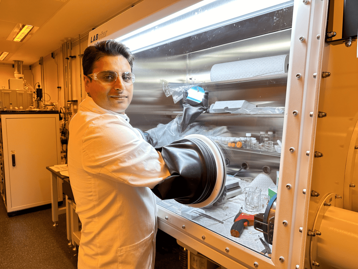
Engineering researchers have developed a 2D printing process using liquid metals that they say could create new ways of creating more advanced and energy efficient computing hardware that is manufactured at the nano scale.
The process comes amid increasing worldwide demand for memory devices, which require significant amounts of energy to produce and use.
“Reducing the temperature at which zirconium and hafnium become liquid is crucial to developing lower-cost electrical devices as far less energy is required,” said Dr Mohammad Ghasemian, the study’s lead author from the School of Chemical and Biomolecular Engineering.
University of Sydney engineers and researchers first combined tin, zirconium and hafnium in a precise ratio. This enabled the alloy to be melted below 500 degrees, far lower than the individual melting points for zirconium (1855 degrees) and hafnium (2227 degrees). The process is documented in Small.
The liquid metal alloy has a thin oxide layer or ‘crust’ while maintaining a liquid centre. It is used to harvest the ultra-thin tin oxide nanosheets doped with hafnium zirconium oxide.

Nano, quantum win science awards
“Tin is abundant, low cost and can be used at a large scale for the manufacture of critical semiconductors, transistors and memory chips,” says Ghasemian.
“Though hafnium zirconium oxide is a well-known ferroelectric material used in nanoscale applications, like memory devices and sensors, obtaining nanosheets using conventional techniques is difficult and costly,” he said.
Applying the tin-zirconium-hafnium alloy allowed the team to harvest the nanothin tin oxide layer doped with hafnium zirconium oxide through exfoliation – lifting it from its liquid surface – so it could then be 2D printed on a substrate as ferroelectric nanosheets. These sheets are designed to form the basis of next generation computing hardware, from semiconductors to memory chips.
“Think of it like a marble coated in ink,” Dr Ghasemian said. “The alloy is like a solvent that allows us to remove that ink and then use it for printing. Our process allows us to harvest this precious crust layer and turn it into ultra-thin sheets, which are then used to manufacture electronics.”
“It could be a new source of functional 2D materials which are not accessible by conventional methods. This process allows us to introduce ferroelectricity into much smaller, 2D metal oxides, allowing for the development of next generation nanoelectronics at low temperatures.”
First published at University of Sydney news

Are you interested in the energy industry and the technology and scientific developments that power it? Then our email newsletter Energise is for you. Click here to become a subscriber.